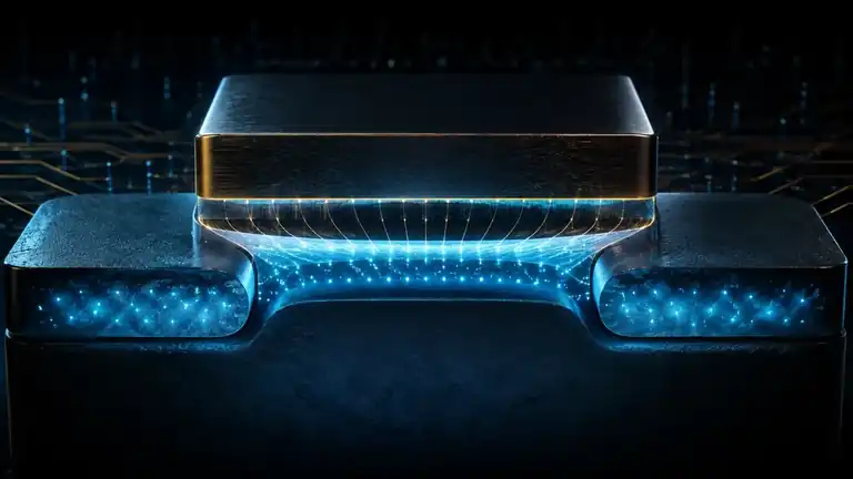
In 1959, a semiconductor problem that had frustrated field-effect transistor designs for decades finally became tractable. At Bell Telephone Laboratories, Mohamed M. Atalla and Dawon Kahng built the first successful insulated-gate field-effect transistor using a stack of metal, silicon dioxide and silicon. That metal–oxide–semiconductor structure gave the device its name: MOSFET.
The importance of the result was not obvious at the time. The first devices were slow, Bell Labs saw no urgent telephone-system application, and early MOS fabrication suffered from instability and contamination. Yet the new structure had a property that bipolar transistors could not match in the same way: a gate electrode could control a conducting channel electrostatically through an insulating oxide, with almost no steady input current. That architecture later proved unusually simple to shrink, replicate and integrate.
Before the MOSFET: a good idea blocked by the surface
Field-effect transistors were not a new idea in 1959. Julius Lilienfeld had patented field-effect concepts in the 1920s, Oskar Heil proposed related structures, and William Shockley investigated field-controlled devices after the invention of the transistor. The conceptual goal was attractive: instead of injecting current into a base region, use an electric field to change the conductivity of a semiconductor channel.
The practical obstacle was the semiconductor surface. A real silicon surface contains dangling bonds, defects and charge traps. These surface states can capture charge and screen the electric field that an external gate is supposed to impose. If the gate field is lost in uncontrolled interface charge, the surface carrier density cannot be modulated predictably.
Atalla's surface-physics work showed that thermally grown silicon dioxide, SiO2, could stabilize and passivate the silicon surface. The oxide was not merely a protective coating: controlling the Si/SiO2 interface removed a central obstacle to field-effect operation. Kahng then used the structure to build a working insulated-gate device in 1959. The associated patent, US 3,102,230, was filed on 31 May 1960 and issued in 1963.
The device architecture
A simplified MOSFET contains four essential elements:
| Element | Function |
|---|---|
| Silicon substrate | semiconductor body in which the channel forms |
| Source and drain | doped regions that inject and collect carriers |
| Thin SiO2 layer | electrically isolates the gate while transmitting its electric field |
| Gate electrode | changes the surface potential and therefore the channel conductivity |
The oxide makes the gate a capacitor rather than a current-injecting contact. Its capacitance per unit area is approximately
Cox = epsilon_ox / t_ox,
where epsilon_ox is the dielectric permittivity and t_ox the oxide thickness. A thinner or higher-permittivity dielectric gives stronger electrostatic coupling, subject to leakage and reliability constraints.
For an enhancement MOSFET, when the gate-to-source voltage exceeds a threshold VT, the surface carrier population can invert and create a conducting channel. In the simplest long-channel model, the inversion charge per unit area scales approximately as
Qinv ≈ -Cox (VGS - VT).
That channel connects source and drain. In the ideal saturation regime, a basic square-law model gives
ID ≈ (1/2) mu Cox (W/L) (VGS - VT)^2,
with carrier mobility mu and device width-to-length ratio W/L. Modern nanoscale transistors deviate strongly from this elementary model, but the causal chain remains recognizable: gate voltage → surface potential → channel charge → drain current.
What changed scientifically
Before Atalla and Kahng, field-effect control of a semiconductor surface was conceptually known but difficult to realize reproducibly in silicon. After their work, the insulated gate became a practical device principle. The breakthrough therefore had two inseparable parts:
- interface physics — reducing the surface-state problem at Si/SiO2;
- device engineering — using that controlled interface as the active gate dielectric of a transistor.
The result turned the oxide from a passive protective material into a functional component that controlled the electronic state of the silicon underneath it.
Why the first MOSFET did not immediately win
The historical outcome was not predetermined. The early MOS transistor was slower than contemporary bipolar devices and had no obvious high-value Bell System application. MOS processing also proved difficult to stabilize. Charges in the oxide and contamination—especially mobile ions such as sodium—shifted threshold voltages and made device characteristics drift.
RCA, Fairchild and other groups continued the work. Researchers including Steven Hofstein, Fred Heiman, Chih-Tang Sah, Bruce Deal, Andrew Grove and Ed Snow helped characterize oxide behavior, contamination and reliability. The later success of MOS was therefore not the work of two people alone; Atalla and Kahng created the decisive device principle, while many teams made the process manufacturable.
From one transistor to integrated circuits
The structural simplicity of MOS became its strategic advantage. The insulated gate drew very little steady current, devices could be packed closely, and planar manufacturing could reproduce enormous numbers of similar transistors.
The progression was rapid once the fabrication problems began to yield:
- 1959 — Atalla and Kahng build the first working MOS field-effect transistor at Bell Labs.
- 1960 — the device is publicly demonstrated and Kahng files the patent that becomes US 3,102,230.
- 1961–1962 — RCA and other laboratories build MOS transistors and experimental multi-transistor structures.
- 1963 — Frank Wanlass proposes complementary MOS, or CMOS, pairing n-channel and p-channel devices so that static power can approach zero in a stable logic state.
- 1964 — General Microelectronics introduces the first commercial MOS integrated circuit, a 20-bit shift register using 120 p-channel transistors.
- late 1960s onward — improved oxide control and manufacturing reliability allow MOS to become a dominant route to large-scale integration.
The key point is causal: the first MOSFET did not itself contain modern computing. It created a transistor architecture whose electrostatic control, low gate current and manufacturing geometry were unusually compatible with repeated scaling.
Why MOS scales so well
A bipolar transistor relies on carrier injection across junctions and needs base current. A MOSFET's insulated gate primarily controls charge by electric field. That gives extremely high input impedance and makes logic gates easier to connect without large steady drive currents.
With CMOS, the power advantage became more decisive. Ideally, one of the complementary transistors is off in a stable logic state, so the direct DC path from supply to ground is nearly eliminated. Dynamic charging of capacitances still consumes energy, and modern leakage is far from zero, but the CMOS principle enabled far denser logic within practical power budgets than a simple scaling of many competing families would have allowed.
The basic switching-energy scale is roughly
E ≈ C V^2,
which makes reductions in node capacitance C and supply voltage V central to low-power digital scaling. This relationship did not emerge from the 1959 device alone, but the MOS gate structure made that scaling trajectory possible.
What the historical breakthrough did not solve
The 1959–1960 MOSFET should not be projected backward as if it already solved modern semiconductor engineering. It did not solve:
- oxide reliability over decades of field stress;
- threshold-voltage control in mass production;
- sodium and other contamination;
- high-density lithography;
- short-channel effects;
- interconnect delay and power;
- modern high-k dielectrics and metal gates;
- FinFET and gate-all-around electrostatics.
Those are later layers of the technology stack. The historical delta was more fundamental: a controllable insulated gate on silicon became a working transistor.
Legacy
The MOSFET eventually became the core switching device of digital integrated electronics. Microprocessors, memory, image sensors, power-management circuits and countless mixed-signal systems descend from the MOS device family. Modern transistors may use metal gates, high-k dielectrics and three-dimensional channels rather than the planar metal/SiO2/silicon geometry of 1959, but the operating abstraction remains recognizably MOS: an insulated gate electrostatically controls a semiconductor channel.
Atalla and Kahng's achievement is therefore not simply another transistor invention. It is the point at which surface chemistry, dielectric physics and semiconductor electrostatics were combined into an architecture that could later be manufactured by the billions on individual chips.
Evidence status
Established historical milestone · primary patent record available · institutional chronology and later semiconductor histories corroborate the 1959 working device and 1960 demonstration/patent sequence.
The precise attribution is best stated as a chain: Atalla's silicon-surface passivation work enabled the controlled Si/SiO2 interface; Kahng fabricated the working MOS field-effect device with Atalla at Bell Labs; later teams transformed that laboratory device into reliable commercial MOS and CMOS technology.
Sources
- https://patents.google.com/patent/US3102230A/en
- https://www.computerhistory.org/siliconengine/metal-oxide-semiconductor-mos-transistor-demonstrated/
- https://patents.google.com/patent/US2961354A/en
- https://patents.google.com/patent/US3206670A/en
- https://www.computerhistory.org/siliconengine/first-commercial-mos-ic-introduced/
- https://www.computerhistory.org/siliconengine/complementary-mos-circuit-configuration-is-invented/