Correção — 14 de outubro de 2026. Esta revisão corrige a cronologia e as atribuições, substitui referências insuficientemente ligadas às afirmações e remove cálculos de taxas de falha sem respaldo e a comparação enganosa entre dimensões históricas e o nome de um nó moderno.
De componentes separados a um circuito
Um transistor controla a corrente; resistores e capacitores exercem outras funções. Sua combinação forma um sistema eletrônico útil. A dificuldade era produzir com confiabilidade tanto os componentes quanto suas conexões.
Em 12 de setembro de 1958, Jack Kilby, da Texas Instruments, demonstrou um oscilador montado com elementos semicondutores de germânio e conexões finas de ouro. Estabeleceu uma via prática para circuitos semicondutores, mas seus fios suspensos não constituíam um processo de interconexão escalável. Sua patente US3138743 descreve elementos ativos e passivos em material semicondutor. Uma patente descreve um projeto e reivindicações; por si só, não mede o rendimento de fabricação.
Marcos: demonstrações e depósitos de patentes
| Marco | Contribuição |
|---|---|
| 1958 — Kilby | Demonstração de um circuito semicondutor funcional |
| 1959 — Hoerni | Processo planar que conserva óxido protetor sobre as bordas das junções; US3025589 depositada em 1 de maio de 1959 |
| 1959 — Noyce | Conexões metálicas sobre óxido isolante; US2981877 depositada em 30 de julho de 1959 |
| 1960 — Equipes Fairchild | Circuitos monolíticos funcionais e desenvolvimento do isolamento entre componentes |
O processo posterior de Hoerni não pode ser requisito do experimento anterior de Kilby. Noyce usou a via planar para resolver as interconexões. As contribuições trataram problemas relacionados; não foram uma única invenção de uma única pessoa.
Por que o óxido importa
A dopagem modifica o comportamento elétrico de regiões selecionadas. Uma junção p–n conecta uma região do tipo p, com lacunas como portadores majoritários, a uma região do tipo n, com elétrons como portadores majoritários. Hoerni conservou óxido de silício sobre as bordas superficiais das junções, em vez de deixá-las expostas.
Noyce usou o óxido como isolante sob trilhas metálicas. Aberturas localizadas permitem contato com regiões semicondutoras sem curto-circuitar junções intermediárias. Isolar as conexões na superfície não isola automaticamente os componentes dentro do silício: isso exige engenharia adicional.
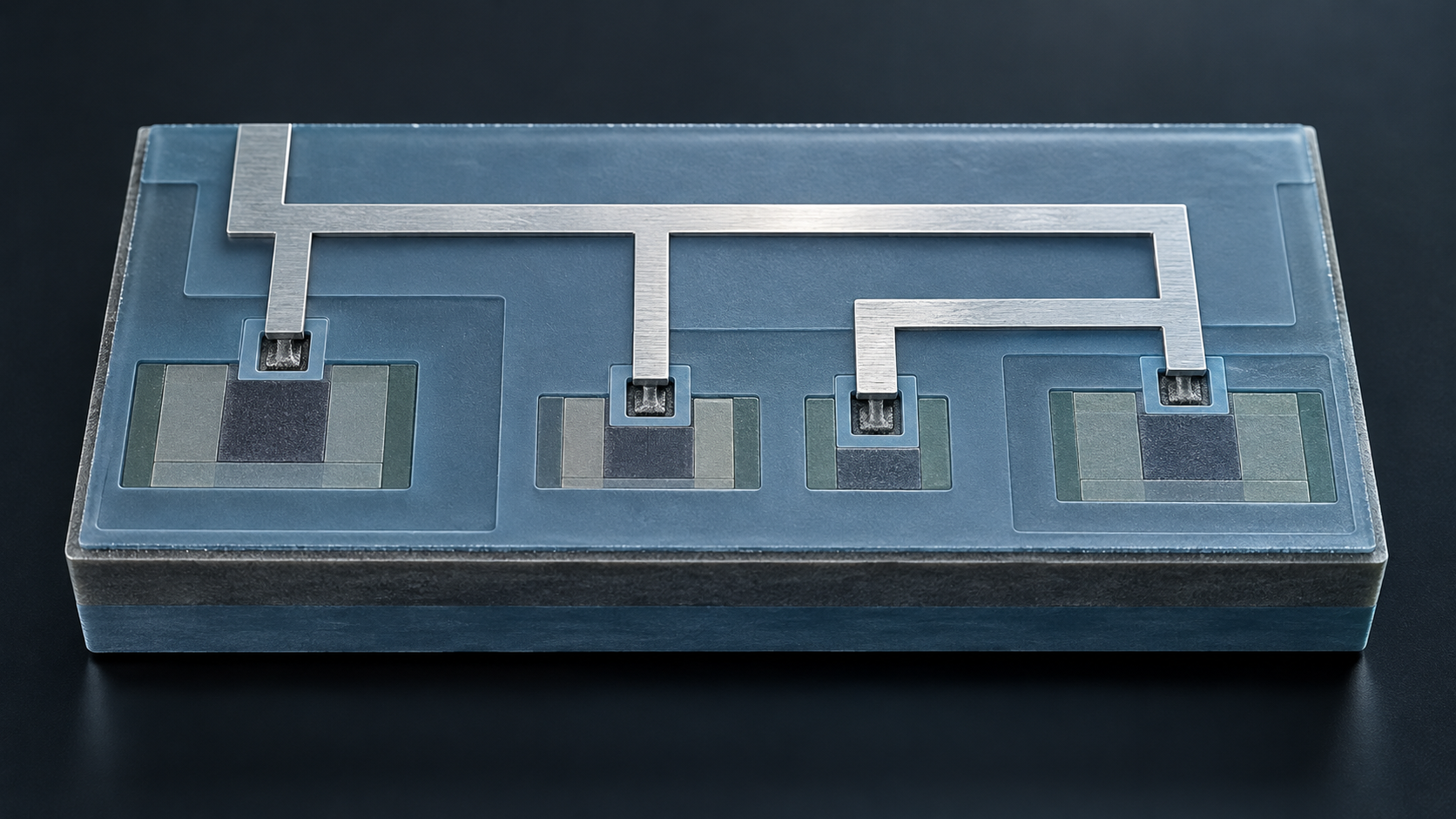
O processo combina definição de padrões, difusão, aberturas de contato e metalização. Fabricar pela mesma face não significa concluir tudo em uma única operação litográfica. A capa ilustra metal sobre isolante; não representa um dispositivo histórico nem um esquema elétrico funcional.
Métodos, evidências e limitações
As descrições e reivindicações das patentes citadas foram examinadas junto com a cronologia do Computer History Museum. O museu distingue o isolamento físico inicial do isolamento posterior por junções nos circuitos Fairchild. Esta reconstrução não relata experimento com semicondutores, fabricação ou replicação de confiabilidade.Os registros conservados sustentam a cronologia e os mecanismos. Não fornecem uma medição comum que demonstre ganho numérico de confiabilidade para cada circuito antigo. Nomes de nós modernos não são diretamente comparáveis a dimensões históricas; essa comparação não é feita aqui. A integração permitiu eletrônica cada vez mais complexa por meio de trabalhos posteriores em materiais, isolamento, fabricação e projeto.
A IA auxiliou esta correção científica e suas traduções; verificações automatizadas não constituem revisão humana. A capa gerada é uma ilustração conceitual. A revisão anterior permanece no histórico editorial.